jeff_rigby
Banned
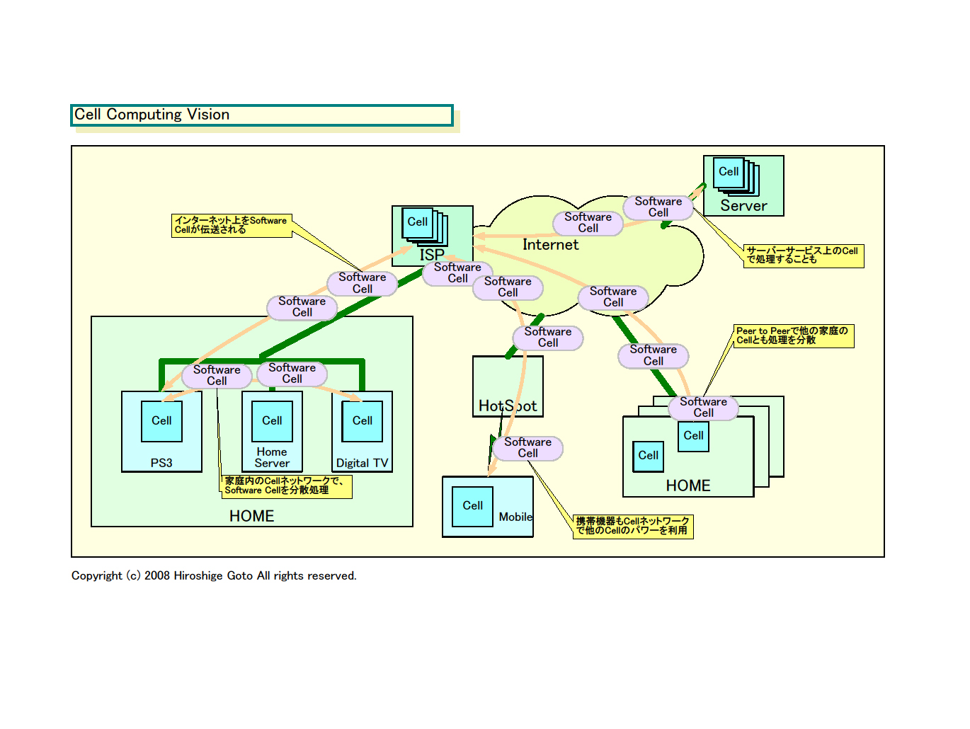
It all starts here in this 2001 paper outlining the future of the CE industry and digital TV. It continues below with hardware and standards development to support what's outlined in the 2001 paper. Read this 2010 article from AMD, Part the Clouds: AMD Fusion APUs Ideal for Cloud Clients and this continuation of the article. Lots there that applies to us and it's an easy read. After reading think about Zlib having hardware support in AMD APUs and the W3C supporting WebCL and Zlib compression as the standards to be used by web browsers. Think about AMD also including a ARM A5 for DRM and more in their APUs.
Next generation Game Console Technology & PC & Handheld & Super Computer:
1) Fusion HSA and Fabric memory Model Scales from Handheld to Super computer Provides efficiencies to reduce heat and increase performance. (includes OpenCL)
2) Third generation 3D stacking making SOCs affordable (SOCs provide more efficiencies = to two die shrinks, reduce time to market) and here 2012-2013.
3) 3D wafer stacked memory will be ready for Game Consoles 2013-2014 Provides even more efficiencies when inside the SOC.
4) Comprehensive look for faster memory technologies and when they would be ready
5) Early draft of the Xbox 720 & Xbox360 marketing and design (from 2010)
Combine all the above and Next generation Game consoles are possible. It must have the performance of a next generation console and fit in the power envelope as well as be affordable. Many consider this an impossible task. Not discussed is the CPU type or version of GPU.
Cites:
Sony CTO interview on Playstation tech
Article on PS4 leaks parallels Sony CTO interview but adds AMD Fusion
Game Console SOCs shown using 3D stacked/ultrawide with TSVs memory (faster, eventually cheaper & energy efficient) and 3D ultra wide I/O memory
AMD planning 5 years for 3D stacking but not mentioning it.
Video on Fusion by AMD
Heterogeneous computing here now.
Cell vision is like HSA + Fabric computing & very attractive to Sony. Everything in the Sony CTO interview about future Playstation tech has been touched on in the above cites. My opinion is the Cell design was an early attempt at this and much has been developed since. Early Cell is not compatible with current open source HSA & Fabric computing memory model, for this reason we will not see Cell but might see SPUs in some form.
OBAN Japanese Coin

The idea of the OBAN, a large blank substrate, to produce a large SOC. It can be custom configured and could be used in the PS4 and Xbox 720. This plus standardized building blocks produced by the consortium make sense. It makes sense of the various rumors. Arguments that this would be ready for this Cycle 2013-2014 have supporting cites.
Old design and assembly methods for SOC with their associated lead times no longer apply. 3D and 2.5D stacking is making large Chips like Memory and FPGA economically practical by splitting up the chip into smaller parts that are checked before assembly in a 3D stack or on 2.5D substrate.
Edit: Going through the SimiAccurate forum and found this:
AMD Process Optimized building blocks includes custom memory (from AMD) and cites I posted confirm Micron developed Custom memory for AMD to include in next generation game consoles; the picture confirms Stacked memory, most likely 256 or 512 ultra wide I/O. Stacked memory in the PS4 SOC is possible, the picture proves it.
Arguments? All the above are hindsight, developed in various discussions on NeoGAF with very good criticisms and supported with cites. My opinion is that AMD and Foundries need game console volumes to kickstart the new technologies and Game consoles need the new technologies to make them practical.
1) microsoft-sony.com
2) digitimes PS4 rumor (Must be a PS3 that was confused with a PS4)
3) Leaked Xbox 720 powerpoint document from 9/2010 which has the Xbox 361 coming this 2012 season. IF Oban 12/2011 then 9/2010 was after it was in the pipeline to be produced.
4) This patent and the timing in both filing and publishing XTV game support.
5) Both ps3 and Xbox 360 refresh must have a price reduction built in to allow a price reduction when the PS4 and Xbox 720 are released. This is already possible for the Xbox 360 but the PS3 would NEED a massive redesign to put both CPU and GPU on the same silicon.
6) Sony 2010 1PPU4SPU patent
7) Elizabeth Gerhard's Projects (IBM employee) and an International project involving the Xbox 360 @ 32nm and NO design work for a PS3 refresh at 32nm
8) Oban = large blank Japanese Coin => Is Oban for both the PS3 and Xbox 361 (Microsoft making the chip for Sony using 1PPU3SPU CPU packages instead of just PPUs )
9) Both having browsers at the same time for the first time ever and both have a refresh at the same time for the first time ever
10) Sony depth camera patent (Timing, 9/2011 & again 2/2012)
11) Khronos Openmax 1.2 (Supports Gstreamer-openmax and camera, second Khronos Pdf mentioning Augmented Reality starting Sept 2012 leveraging the browser libraries
12) ATSC 2.0 *-* starts May 2012 thru 1st quarter 2013. *-* h.265 published for use Jan 2013. *-* Sony Nasne *-* RVU support for the PS3 announced by Verizon and Direct TV
13) Energy Star third tier game console voluntary requirements
14) Information on Next generation game console technology
15) Tru2way RVU and the Comcast RDK
http://pc.watch.impress.co.jp/docs/2009/0226/kaigai492.htm
Feb 2009 : Sony investigating two PS4 options Super CELL and Larrabee
http://pc.watch.impress.co.jp/docs/column/kaigai/20091224_339258.html
Dec 2009 : Sony picks Super CELL option for PS4.
http://pc.watch.impress.co.jp/docs/column/kaigai/20100309_353492.html
March 2010 : Additional Description of Super CELL. Interestingly, Sony was most serious about going Larrabee.
http://pc.watch.impress.co.jp/docs/column/kaigai/20120608_538586.html
June 2012 : Super CELL plan died by the end of 2010. SCEI picks AMD in 2011.
________________________________________________________________________________________
"For future reference, the next links a that are merely quotes of Jeff Rigby will be deleted without comment and result in infractions or temp-bans." on Beyond 3D.
Next generation Game Console Technology & PC & Handheld & Super Computer:
1) Fusion HSA and Fabric memory Model Scales from Handheld to Super computer Provides efficiencies to reduce heat and increase performance. (includes OpenCL)
2) Third generation 3D stacking making SOCs affordable (SOCs provide more efficiencies = to two die shrinks, reduce time to market) and here 2012-2013.
3) 3D wafer stacked memory will be ready for Game Consoles 2013-2014 Provides even more efficiencies when inside the SOC.
4) Comprehensive look for faster memory technologies and when they would be ready
5) Early draft of the Xbox 720 & Xbox360 marketing and design (from 2010)
Combine all the above and Next generation Game consoles are possible. It must have the performance of a next generation console and fit in the power envelope as well as be affordable. Many consider this an impossible task. Not discussed is the CPU type or version of GPU.
Cites:
Sony CTO interview on Playstation tech
Article on PS4 leaks parallels Sony CTO interview but adds AMD Fusion
Game Console SOCs shown using 3D stacked/ultrawide with TSVs memory (faster, eventually cheaper & energy efficient) and 3D ultra wide I/O memory
AMD planning 5 years for 3D stacking but not mentioning it.
Video on Fusion by AMD
Heterogeneous computing here now.
Cell vision is like HSA + Fabric computing & very attractive to Sony. Everything in the Sony CTO interview about future Playstation tech has been touched on in the above cites. My opinion is the Cell design was an early attempt at this and much has been developed since. Early Cell is not compatible with current open source HSA & Fabric computing memory model, for this reason we will not see Cell but might see SPUs in some form.
This is starting in 2012 with full production scheduled for 2013. It makes sense given standardized building blocks mentioned above in the quote to have a design tool in place to make a blank substrate (Oban) with bumps and traces to allow the building blocks to be attached. This can reduce the time to market and allow for tweeking the design which must be the case as there are rumors of the Oban 720 chip being produced Dec 2011 but redesign rumors last month. This is not possible any other way.http://eda360insider.wordpress.com/2011/12/14/3d-week-driven-by-economics-its-now-one-minute-to-3d/ said:According to the data gleaned from presentations by Samsung, Toshiba, AMD, and others, 3D IC assembly gives you the equivalent performance boost of 2 IC generations (assuming Dennard scaling wasn’t dead). Garrou then quoted AMD’s CTO Byran Black, who spoke at the Global Interposer Technology 2011 Workshop last month. AMD has been working on 3D IC assembly for more than five years but has intentionally not been talking about it. AMD’s 22nm Southbridge chips will probably be the last ones to be “impacted by scaling” said Black. AMD’s future belongs to partitioning of functions among chips that are process-optimized for the function (CPU, Cache, DRAM, GPU, analog, SSD) and then assembled as 3D or 2.5D stacks.
OBAN Japanese Coin
The idea of the OBAN, a large blank substrate, to produce a large SOC. It can be custom configured and could be used in the PS4 and Xbox 720. This plus standardized building blocks produced by the consortium make sense. It makes sense of the various rumors. Arguments that this would be ready for this Cycle 2013-2014 have supporting cites.
Old design and assembly methods for SOC with their associated lead times no longer apply. 3D and 2.5D stacking is making large Chips like Memory and FPGA economically practical by splitting up the chip into smaller parts that are checked before assembly in a 3D stack or on 2.5D substrate.
Edit: Going through the SimiAccurate forum and found this:
The PS4 SOC should have 100 megs or so of VERY VERY fast "common" memory in the SOC. It's possible to have more, to have the entire system memory in the SOC. This is not likely though if the second GPU is external and also Full HSA using a GDDR memory buss rather than PCIe.http://semiaccurate.com/forums/showpost.php?p=158494&postcount=139 said:AI technique such as Neural Network(image, handwriting recognition) and Genetic Algorithm(optimization used in planning) basically performs searches in parallel. AI techniques are best implemented in a system with many cores. A 1K nodes Neural Network or a Genetic Algorithm with 1K population size will perform 1K searches in parallel. These algorithms do not need a lot of memory. 100MBytes of memory is should be more than enough. What AI algorithm needs is more processing cores.
Currently, the GPU and CPU does not have a common address space. The algorithm needs to move the memory between the GPU and CPU many times during the execution. The memory swaps make implementation of AI on GPU not very efficient. Once the GPU and CPU share the same memory space, it will be very efficient to implement AI on GPU.
If GPU and CPU share the same memory space in Kaveri, Kaveri will have great impact how software is implemented. AI, Computer Vision and linear programming implemented on GPU will be many times faster than implemented on CPU. There will be alot more AI and Computer Vision application on the laptop.
"Orbis will support 4 layer BR discs from day 1" most likely means that Orbis will be a 4K blu-ray player also (4 layer + h.265= 4K Blu-ray) All PS3s can support 4K video but only Slim blu-ray drives may be able to read 4 layers. (To not fragment the PS3, Sony may not enable 4K blu-ray on the PS3.)http://www.forum-3dcenter.org/vbulletin/showthread.php?p=9241544#post9241544 said:Spec numbers that IGN posted are from first/early dev kits that have been replaced in mid January. Now I repeat what I know is based on second dev kits that DO NOT represent the final product. Kits will mosT definitely change. Before I reveal SOME of the specs let me tell you that based on what we have heaRd in our studio from our publisher is that Sony was undecided if they should go for a high end machine and take On MS or go for 1.5 leap.
According to rumors a couple of Sonys first party studios are asking for high end machine to make games that are going to have noticeable generation leap. While Hirai and other heads over in Japan think it's time to think about profitability. For now "fight" is some where in between, edging more towards higher end. RAM has been raised from 2GB to 4GB when most of bigger publishers and first party studios that have saying went mental.CPU yes it is true Sony is moving away from the CELL. Will there be BC? Our publisher doesn't care and we haven't heard a word about it. Again since these are dev kits we can't know more than that 99% ceLL is done and dusted. Second dev kit uses APU design AMD A8-3870k redesigned to have HD 6850 on board. And yes SI rumors are true. APU is paired with the HD Radeon HD 7900. No HDD rumors are untrue since it has aLready been confirmed that just like PS3, every "Orbis" SKU will have large HDD since Sony is very eager to make Orbis the media hub. O and one more thing Orbis will support 4 layer BR discs from day 1."
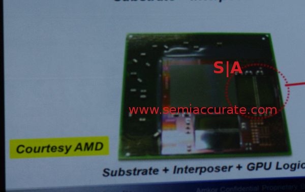
Stacked Memory plus GPU plus substrate. Two of the 4 CUSTOM memory chips are in the red dotted circle (could be total 256 or 512 bit wide). This is the same 2.5D substrate + Interposer technology we will probably see supporting the PS4 SOC just with PS4 SOC much LARGER. It also looks like the following picture includes Southbridge. Just missing the CPUs and MMU for CPU and it would be a APU including memory.http://semiaccurate.com/forums/showpost.php?p=164227&postcount=225 said:That's why I keep posting 2.5D stacking news released by the company that Charlie's "Far Future AMD GPU Prototype" picture originated from. Moreover, Charlie made it rather clear that SONY is going for a "multi-chip-on-interposer" HSA design that is supposed to be gradually integrated into a cheaper, monolithic SoC later in the life cycle. We also heard about "two GPUs", so its probably going to be APU + dedicated GPU - with the APU-GPU basically reserved for GPGPU computation.
"Interposer inclusion defines the 2.5D approach. It will route thousands of interconnections between the devices. Coupled with true 3D stacked die (enabled by TSVs), the high routing density and short chip-to-chip interconnect ensures the highest possible performance while packing as much functionality as possible into the smallest footprint.
Functional blocks may include a microprocessor or special purpose logic IC (GPU, applications processor, ASIC, FPGA, etc.) connected through high-speed circuitry to other logic devices or memory (DRAM, SRAM, Flash) ..."
AMD Process Optimized building blocks includes custom memory (from AMD) and cites I posted confirm Micron developed Custom memory for AMD to include in next generation game consoles; the picture confirms Stacked memory, most likely 256 or 512 ultra wide I/O. Stacked memory in the PS4 SOC is possible, the picture proves it.
Arguments? All the above are hindsight, developed in various discussions on NeoGAF with very good criticisms and supported with cites. My opinion is that AMD and Foundries need game console volumes to kickstart the new technologies and Game consoles need the new technologies to make them practical.
1) microsoft-sony.com
2) digitimes PS4 rumor (Must be a PS3 that was confused with a PS4)
3) Leaked Xbox 720 powerpoint document from 9/2010 which has the Xbox 361 coming this 2012 season. IF Oban 12/2011 then 9/2010 was after it was in the pipeline to be produced.
4) This patent and the timing in both filing and publishing XTV game support.
5) Both ps3 and Xbox 360 refresh must have a price reduction built in to allow a price reduction when the PS4 and Xbox 720 are released. This is already possible for the Xbox 360 but the PS3 would NEED a massive redesign to put both CPU and GPU on the same silicon.
6) Sony 2010 1PPU4SPU patent
7) Elizabeth Gerhard's Projects (IBM employee) and an International project involving the Xbox 360 @ 32nm and NO design work for a PS3 refresh at 32nm
8) Oban = large blank Japanese Coin => Is Oban for both the PS3 and Xbox 361 (Microsoft making the chip for Sony using 1PPU3SPU CPU packages instead of just PPUs )
9) Both having browsers at the same time for the first time ever and both have a refresh at the same time for the first time ever
10) Sony depth camera patent (Timing, 9/2011 & again 2/2012)
11) Khronos Openmax 1.2 (Supports Gstreamer-openmax and camera, second Khronos Pdf mentioning Augmented Reality starting Sept 2012 leveraging the browser libraries
12) ATSC 2.0 *-* starts May 2012 thru 1st quarter 2013. *-* h.265 published for use Jan 2013. *-* Sony Nasne *-* RVU support for the PS3 announced by Verizon and Direct TV
13) Energy Star third tier game console voluntary requirements
14) Information on Next generation game console technology
15) Tru2way RVU and the Comcast RDK
http://pc.watch.impress.co.jp/docs/2009/0226/kaigai492.htm
Feb 2009 : Sony investigating two PS4 options Super CELL and Larrabee
http://pc.watch.impress.co.jp/docs/column/kaigai/20091224_339258.html
Dec 2009 : Sony picks Super CELL option for PS4.
http://pc.watch.impress.co.jp/docs/column/kaigai/20100309_353492.html
March 2010 : Additional Description of Super CELL. Interestingly, Sony was most serious about going Larrabee.
http://pc.watch.impress.co.jp/docs/column/kaigai/20120608_538586.html
June 2012 : Super CELL plan died by the end of 2010. SCEI picks AMD in 2011.
________________________________________________________________________________________
"For future reference, the next links a that are merely quotes of Jeff Rigby will be deleted without comment and result in infractions or temp-bans." on Beyond 3D.