You are using an out of date browser. It may not display this or other websites correctly.
You should upgrade or use an alternative browser.
You should upgrade or use an alternative browser.
The Verge: Nvidia to release RTX 5070 and 5090 in January, announcmeent at CES 2025
MrTroubleMaker
Member

SweetTooth
Gold Member

OverHeat
« generous god »
That it's going to suck at RT compared to nvidia sure!
Magic Carpet
Gold Member
I still don't understand how they get all those tiny wires hooked into the chip itself. I've seen a video of a machine doing it and all I could see was what looked like tiny wispy strings of hot metal blowing around and suddenly all the wires are connected.
Buggy Loop
Gold Member
I still don't understand how they get all those tiny wires hooked into the chip itself. I've seen a video of a machine doing it and all I could see was what looked like tiny wispy strings of hot metal blowing around and suddenly all the wires are connected.
? The interface between the PCB and the chipset? They don't use bonding wires on such complex devices, they take too much space and the process complexity goes exponential with how complex the chipset is.
They use BGA, ball grid arrays, soldering balls to make contacts
We see it a bit here in this 4090 reballing video (insane job to do manually)
Or you meant something else?
Magic Carpet
Gold Member
? The interface between the PCB and the chipset? They don't use bonding wires on such complex devices, they take too much space and the process complexity goes exponential with how complex the chipset is.
They use BGA, ball grid arrays, soldering balls to make contacts
We see it a bit here in this 4090 reballing video (insane job to do manually)
Or you meant something else?
I'm talking about under all those balls, they got to connect those balls to the chip itself somehow. Thats what I don't understand.
I'm talking about under all those balls, they got to connect those balls to the chip itself somehow. Thats what I don't understand.
It's not really any different than how the substrate attaches to the PCB, just that the solder balls on the GPU die are much smaller. It's called flip chip.
Last edited:
Magic Carpet
Gold Member
I'm thinking more like this.It's not really any different than how the substrate attaches to the PCB, just that the solder balls on the GPU die are much smaller. It's called flip chip.

Wire bonding - Wikipedia
Wire bonding is for less complex chips because the connection density isn't as high.
Magic Carpet
Gold Member
Thanks, I've been on wikipedia learning about all this morning thanks to the links.Wire bonding is for less complex chips because the connection density isn't as high.
Hohenheim
Member
Hopefully it's only a few weeks apart from the 5080.I am going to be pissed off if we dont get 5090 this Jan. I do not want a 5080 -_-
it looks weak compared to the 5090 by allot.
it doesnt even look more powerful than the 4090. I know it's a different design but Nvidia discontinuing the 4090 means the 5080 is about on par with the 4090 at a much cheaper price. IF i wanted a 4090 level i would have kept my card. I want the next best thing.
cmon Nvidia. 5090.. day one. lets go .
Buggy Loop
Gold Member
I'm talking about under all those balls, they got to connect those balls to the chip itself somehow. Thats what I don't understand.
Micro balls /bumps/pillars, not solder nowadays for the most part but making the interface to the substrate and bonded in epoxy or other exotic bonding techniques


Everything is balls/pillars for interfacing from die to substrate to PCB
As for creating those bumps on silicon

Did that on one hand on cellphone while baby is sleeping on me, sorry if it's barebones hehe, but from that you can search the subjects deeper.
Edit, one of my favourite channel on the die technology, brief history of packaging
Last edited:
iQuasarLV
Member
Micro balls /bumps/pillars, not solder nowadays for the most part but making the interface to the substrate and bonded in epoxy or other exotic bonding techniques
Everything is balls/pillars for interfacing from die to substrate to PCB
As for creating those bumps on silicon
Did that on one hand on cellphone while baby is sleeping on me, sorry if it's barebones hehe, but from that you can search the subjects deeper.
Edit, one of my favourite channel on the die technology, brief history of packaging
Ah, another person of taste I see. =D
Last edited:
Magic Carpet
Gold Member
Micro balls /bumps/pillars, not solder nowadays for the most part but making the interface to the substrate and bonded in epoxy or other exotic bonding techniques
Everything is balls/pillars for interfacing from die to substrate to PCB
As for creating those bumps on silicon
Did that on one hand on cellphone while baby is sleeping on me, sorry if it's barebones hehe, but from that you can search the subjects deeper.
Edit, one of my favourite channel on the die technology, brief history of packaging
I think I'm finally starting to wrap my brain around it. Man, I knew it was a bunch of connections but dang.
Buggy Loop
Gold Member
I think I'm finally starting to wrap my brain around it. Man, I knew it was a bunch of connections but dang.
Modern chipsets are insanely complex yea.
The course I did on semiconductors for electrical engineering was just the basics and everyone had a nose bleed in that course. Let alone modern chips. It's witchcraft

Nothing human made is more complex than this
Breaks my brain even more so when we go into the scales of the silicon die itself.
Speaking of which, really cool video on lithography ASML put out 4 weeks ago
Last edited:
YeulEmeralda
Linux User
She was 4 nanometers you sick fuck!
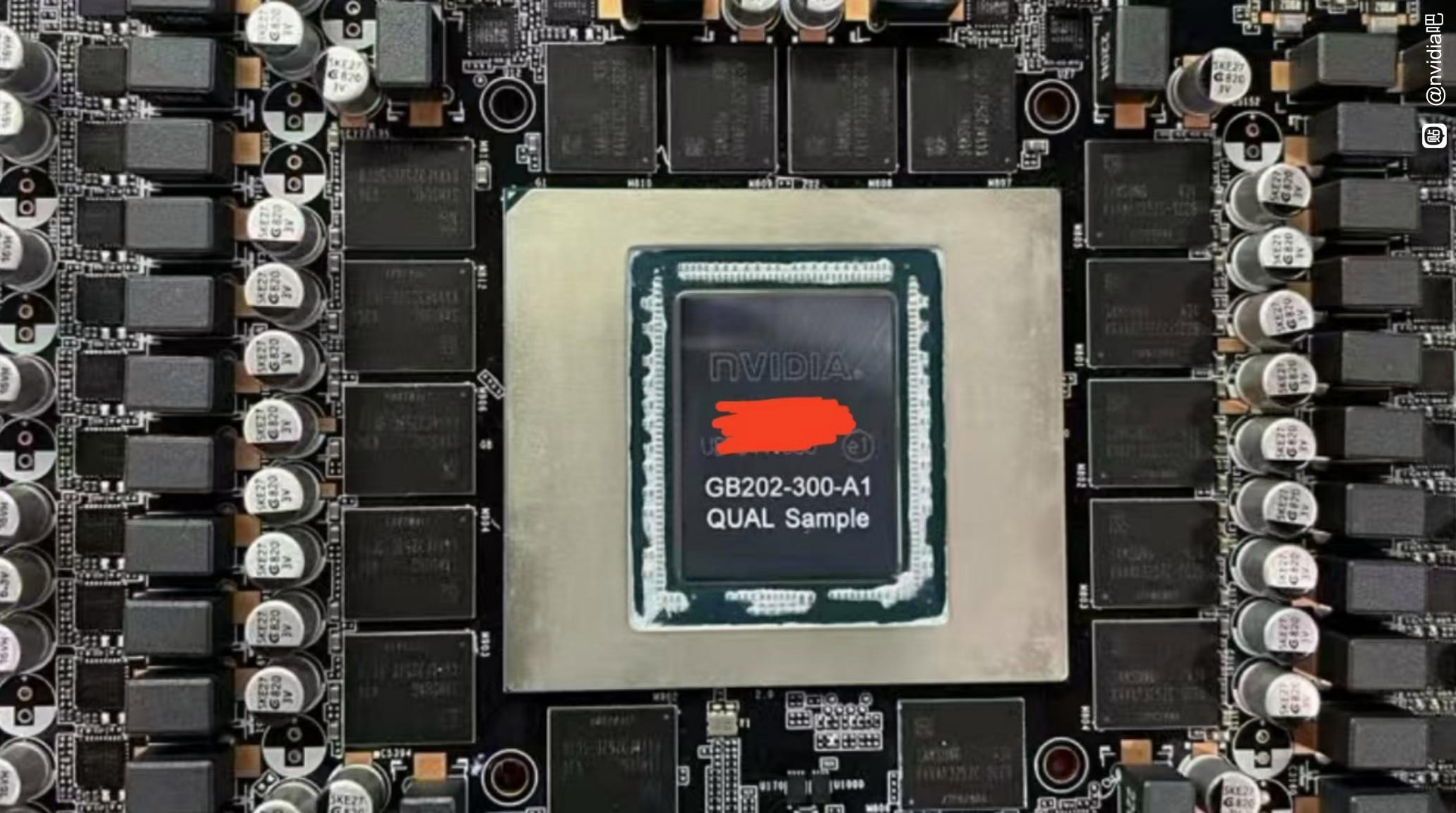
NVIDIA GeForce RTX 5090 to feature 16+6+7 power design and 14-layer PCB!!!
Boom

NVIDIA GeForce RTX 5090 to feature 16+6+7 power design and 14-layer PCB - VideoCardz.com
GeForce RTX 5090 with powerful PCB Benchlife added more details to the RTX 5090 pre-launch rumors. According to the site, which is usually well-informed due to its close contacts with many AIBs, the upcoming flagship Blackwell GPU is said to adopt a 16+6+7 power stage design. For comparison, the...
 videocardz.com
StereoVsn
Gold Member
Asionometry channel is really good for discussions of both modern technology as well as history.I think I'm finally starting to wrap my brain around it. Man, I knew it was a bunch of connections but dang.
Similar threads
- 141
- 12K
SmokSmog
replied